Updated:
VHDL IP: AD7303
Chip Description
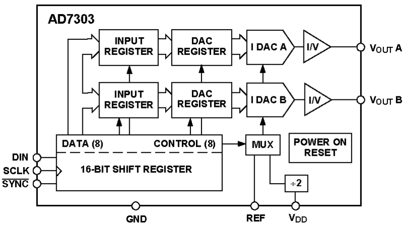
The AD7303 is an 2-channel 8-bit DAC with a SPI interface. Rather than use a complete, general SPI master transceiver, I developed an specific (''ad hoc'') interface logic which is extremely simple and easy to use from PicoBlaze or some system else.
The interface moves two 8-bit samples in 68 system clock cycles so the maximum DAC data rate @50MHz is 50 x 10^6 / 68 = 735.29 kHz for each channel. The predefined configuration for AD7303 (It is possible to use other config modifying the VHDL code, it's no possible use different configurations once the design is implemented) is:
- the two DAC channels enabled
- collect data from the shift register instead from input register
- set the internal reference (Vdd/2)
Ports and Usage
The macro has the following ports:
| Port | DIR | Type | Description |
|---|---|---|---|
| reset | Input | signal | Asynchronous reset |
| clk | Input | signal | Clock signal. Must be lower than 60MHz because ''sclk'' freq. is a half of the ''clk'' freq. and the AD7303 admit a ''sclk'' of 30MHz at maximum |
| wr | Input | signal | Chip enable (write signal). Start the tx operation, ''rdy'' goes low until the macro has finished the tx of two samples (L and R). |
| XL_wr | Input | signal | Chip enable signal for the XL register |
| XR_wr | Input | signal | Chip enable signal for the XR register |
| XL | Input | 8-bit bus | Register that stores the "left" sample (AD7303 is a 2-channel DAC) |
| XR | Input | 8-bit bus | Register that stores the "right" sample (AD7303 is a 2-channel DAC) |
| rdy | Output | signal | Ready signal, while the macro is busy, this signal is 0 |
| int_rdy | Output | signal | Rise one clock cycle pulse when ''rdy'' goes 1 (use it to interrupt PicoBlaze for example) |
| sclk | Output | signal | SPI serial clock signal |
| din | Output | signal | SPI serial data signal |
| sync | Output | signal | SPI chip select signal |
Put data samples on ''XL'' and ''XR'' ports and assert ''XL_wr'' and ''XR_wr'' until the next ''clk'' rising edge, then assert ''wr'' signal until the ''clk'' rising edge. At this moment ''rdy'' goes 0, the sample will be transferred to DAC in 68 clock (''clk'') cycles. Wait ''rdy'' signal to be 1 again, this notifies you that the transmission has finished. See the cronogram below.
Block Diagram And Control State Machine
The figure depicted below shows the RTL block diagram of the circuit. All sequential blocks share the same asyncronous reset and clock signals. The control finite state machine (FSM) has 9 states, there are 6 control signals for datapath. The 4-bits up counter serves to greatly simply the FSM's graph.
Datapath
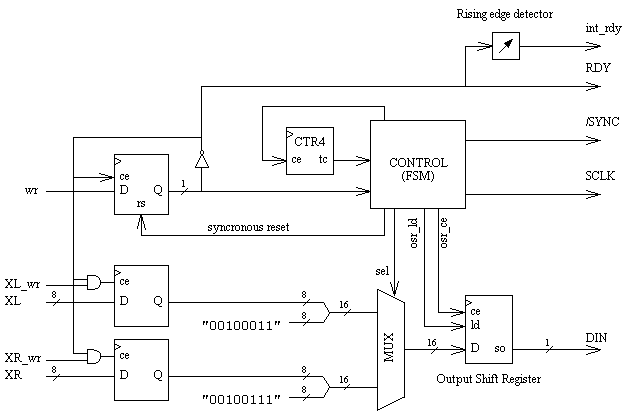
Control

| State | rs | sel | sync | osr_ce | osr_ld | ctr_ce | sclk |
|---|---|---|---|---|---|---|---|
| e00 | 0 | - | 1 | 0 | 0 | 0 | 0 |
| e01 | 0 | 0 | 1 | 1 | 1 | 0 | 0 |
| e02 | 0 | 0 | 0 | 0 | 0 | 1 | 0 |
| e03 | 0 | 0 | 0 | 1 | 0 | 0 | 1 |
| ee | 0 | - | 1 | - | - | 0 | 0 |
| e04 | 0 | 1 | 1 | 1 | 1 | 0 | 0 |
| e05 | 0 | 1 | 0 | 0 | 0 | 1 | 0 |
| e06 | 0 | 1 | 0 | 1 | 0 | 0 | 1 |
| e07 | 0 | - | 0 | 0 | 0 | 1 | 0 |
The FSM has the following graph, state after reset is e0, the control signals in each state are shown in the table. The signals printed in green are registered because random effects on this signals could cause a malfunctioning of entire system (AD7823 expects inputs free of spurious transitions)
Synthesis Report
    Device xc3s400-4ft256

    slice=30
    ff=45
    lut=42
    iob=26
    gclk=1
    mfreq=233.91MHz
Download
- ad7303.vhd
- ad7303_test.vhd. A test bench for simulation
- utils.vhd. A package with some useful routines